Comprehensive Guide to Flash Memory: Architecture, Types, and Products
Flash memory has become a critical component in modern technology, from usb drives to sd cards, playing a key role in data storage solutions. This guide will explore the different types of flash memory, analyze its architecture, and highlight key products in the market. Readers will gain insights into how flash memory works and the advantages it offers, helping to address common storage challenges faced by businesses today. Understanding these concepts can empower users to make informed decisions about their storage solutions, enhancing their overall productivity and efficiency.
Understanding Flash Memory Technology

Flash memory technology plays a crucial role in modern data storage, particularly in its architecture that supports universal flash storage solutions. This section explores its historical development, including key contributions by industry leaders like Intel and insights from the Institute of Electrical and Electronics Engineers. Readers will gain a foundational understanding of how flash storage evolved, achieving sizes in gigabyte capacities to meet growing demands.
Introduction to Flash Memory Architecture
Flash memory architecture is a crucial component of data storage technology, allowing for high-density storage in devices ranging from USB drives to solid-state drives (SSDs). Unlike traditional floppy disks, which relied on magnetic storage, flash memory utilizes memory cells to store data electronically, providing faster access speeds and increased reliability. With advancements in flash memory technology, storage capacities have expanded from the megabyte range to several terabytes, catering to the increasing demands for data in sectors such as technology and media, especially in regions like South Korea, where digital advancements are rapidly evolving.
The architecture of flash memory typically incorporates NAND or NOR structures, each suited for different applications. For instance, NAND flash, commonly used in SSDs, offers optimal space efficiency and performance for reading and writing operations. In contrast, NOR flash provides faster read speeds, making it ideal for applications that require quick data access. As manufacturers integrate ultraviolet technology in the production of these memory chips, feedback from market trends continues to shape future developments in flash memory, ensuring ongoing improvements in data storage solutions.
Historical Development of Flash Memory
The historical development of flash memory traces back to the late 1980s when Dr. Fujio Masuoka of Toshiba first invented this technology. This innovation paved the way for the architectural advancements that enable compact flash memory to be utilized in a wide range of consumer electronics, from cameras to mobile devices. Over the years, the emergence of custom jump drives has showcased how flash memory can cater to the growing storage needs within computer networks, allowing users to transfer large amounts of data efficiently.
In the following decades, major players in the industry, such as Intel and SanDisk, contributed to the evolution of flash memory, enhancing its architecture and performance. Their efforts led to the standardization of various forms, including NAND and NOR flash, further optimizing it for diverse applications. As the demand for high-capacity storage solutions escalated, these developments solidified flash memory’s role in supporting vast computer networks and its position as a cornerstone in modern data storage technology.
Exploring Flash Memory Types
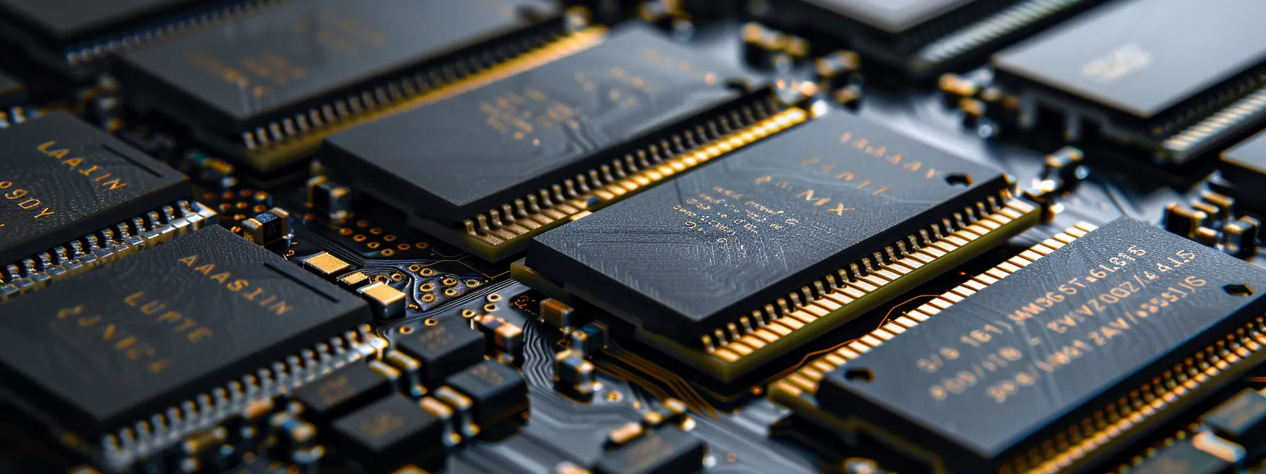
This section provides an overview of various flash memory types that are essential in modern technology. It will cover Single-Level Cell (SLC) architecture, Multi-Level Cell (MLC) configurations, and the characteristics of Triple-Level Cell (TLC) and Quad-Level Cell (QLC) NAND technology. Additionally, insights into 3D NAND technology will illustrate how these advancements enhance storage solutions for devices like cameras and utilize SATA interfaces effectively, while examining their reliance on silicon and electricity.
Single-Level Cell (SLC) Explained
Single-Level Cell (SLC) technology represents one of the most efficient architectures in flash memory, storing a single bit of data per cell. This characteristic allows SLC to achieve higher performance and reliability compared to other configurations, making it an ideal choice for applications in data centers that require rapid access to large volumes of data. With its capabilities to handle demanding workloads, SLC is particularly beneficial for scenarios involving artificial intelligence where low latency and high durability are crucial.
In terms of mass storage, SLC excels by offering enhanced endurance, which translates to a longer lifespan for storage devices. This advantage makes SLC flash memory suitable for environments where consistent performance is necessary, such as in enterprise-level computing. By utilizing this technology, organizations can maximize data throughput while effectively managing byte-level operations across various applications, ensuring that critical information is readily available when needed.
Multi-Level Cell (MLC) Overview
Multi-Level Cell (MLC) technology represents a significant advancement in flash storage, allowing multiple bits of data to be stored per cell. This architecture enhances storage capacity while maintaining cost-effectiveness, making it an appealing choice for various applications, including consumer electronics and enterprise solutions. MLC utilizes an electric field to adjust the state of the memory cells, but it can be more susceptible to wear compared to Single-Level Cell (SLC) configurations, necessitating effective management to prolong the lifespan of devices.
Western Digital has been at the forefront of implementing MLC technology in its products, providing storage solutions that balance performance and affordability. With the rising popularity of Non-Volatile Memory Express (NVMe) interfaces, MLC has seen increased adoption in high-speed applications where quick data access is essential. Businesses seeking efficient storage solutions can benefit from the thoughtful integration of MLC technology, as it offers an optimal blend of performance and capacity for a range of demands.
Triple-Level Cell (TLC) Insights
Triple-Level Cell (TLC) technology is known for its impressive density, allowing three bits of data to be stored in each memory cell. This feature significantly increases the mass storage capacity of devices, making TLC a popular choice for consumer electronics and portable storage solutions. Companies like IBM have utilized TLC technology in their products to meet escalating demands for greater storage without compromising on physical device size.
Although TLC employs a high voltage to achieve its storage capabilities, this can lead to a higher susceptibility to wear over time compared to Single-Level Cell (SLC) and Multi-Level Cell (MLC) architectures. Users seeking reliable yet affordable storage options will find TLC offers an effective solution, especially in settings where large amounts of data, such as images from SmartMedia cards, need to be retained efficiently. As advancements continue, TLC storage remains a vital component in the evolution of flash memory technology.
Quad-Level Cell (QLC) Characteristics
Quad-Level Cell (QLC) technology represents a further advancement in flash memory by allowing four bits of data to be stored in each cell. This capability significantly enhances storage density, making QLC a practical option for high-capacity memory cards and other storage solutions. Companies like Micron Technology have developed QLC products that compete with traditional magnetic storage options, appealing to users who require extensive data storage without the bulk of conventional drives.
Despite its impressive capacity, QLC architecture often necessitates sophisticated firmware to manage its durability effectively. This complexity arises from QLC’s increased susceptibility to wear, resulting from higher data density compared to older flash types. Businesses looking to optimize their storage solutions must weigh the benefits of high capacity against potential longevity issues, understanding that QLC can be a valuable asset in environments where large quantities of data need to be retained efficiently.
3D NAND Technology
3D NAND technology offers a revolutionary approach to data storage by stacking memory cells vertically, which significantly increases density and boosts read and write speeds. This advancement is instrumental for devices such as smartphones and central processing units, as it allows for enhanced virtual memory capabilities that are essential for running multiple applications simultaneously without performance degradation. In Europe, where the demand for compact and efficient storage solutions continues to rise, 3D NAND technology is seen as a key player in meeting these needs while ensuring data security.
The integration of 3D NAND technology not only optimizes physical space within devices but also contributes to improved endurance and longevity of storage products. As manufacturers focus on enhancing data security features alongside performance, businesses can rely on 3D NAND solutions to support critical applications that require swift access to large datasets. This approach allows organizations to keep pace with growing data requirements and fosters an environment where technology serves as a catalyst for efficiency and productivity.
Analyzing Flash Memory Architecture

The analysis of flash memory architecture encompasses several critical components that define its functionality and performance. It will examine how memory cells function in flash, the pivotal role of controllers in managing data flow, and the key architectural differences between NOR and NAND types. Additionally, the layout and design of flash memory, including its integration into it infrastructure and compatibility with technologies like PCI Express and CF cards, will be explored to provide practical insights for users.
How Memory Cells Function in Flash
Memory cells in flash technology operate based on the principle of threshold voltage, which determines the state of each cell. Each cell can represent data by holding an electric charge, with different levels signifying binary values. For instance, in multi-level cell architectures, variations in threshold voltage allow multiple bits to be stored, increasing overall storage density. In Japan, advancements in memory cell design have enhanced the efficiency of compact flash card readers, providing faster data transfer for devices requiring rapid access.
The functionality of memory cells is intricately linked to their architecture and the usage of supportive technologies such as graphics processing units (GPUs). Memory control mechanisms actively manage the storage and retrieval of data, ensuring optimal performance. For example, renowned experts like Dawon Kahng have contributed to refining memory cell structures, leading to breakthroughs in flash storage capabilities. This ongoing evolution assists businesses in developing solutions that efficiently handle vast amounts of data, aligning with modern digital demands.
The Role of Controllers in Flash Memory
The controllers in flash memory play a vital role in managing the flow of data between the computer data storage and the memory cells. They ensure that data is accurately written, read, and erased, maintaining the integrity of the information stored. Effective controllers enhance performance, particularly in applications such as transferring data from an SD card to USB, where speed and reliability are essential for user satisfaction.
Architecture Differences Between NOR and NAND
NOR and NAND flash memory represent distinct architectural designs that serve different purposes in data storage applications. NOR flash allows for random access of data, making it suitable for microcontrollers and scenarios requiring fast read speeds. This architecture’s ability to execute code directly from the memory makes it compatible with programming languages that demand quick responsiveness, such as during cloud computing processes where immediate data retrieval is critical.
In contrast, NAND flash architecture is optimized for higher storage densities and cost-effectiveness, often utilized in solid-state drives and large-scale data storage solutions. Its design relies on algorithms that manage data storage more efficiently, allowing multiple bits to be stored per cell. This makes NAND an ideal choice for applications like bulk data storage where performance in terms of writing and reading large blocks of data holds greater importance than rapid access times, such as in cloud-based infrastructures.
Flash Memory Layout and Design
The layout and design of flash memory are critical in optimizing storage efficiency and performance. CompactFlash cards, for instance, utilize a well-structured array of memory cells arranged in a grid format, ensuring effective use of space while allowing for rapid access to data. Industry leaders like Kioxia focus on refining this architecture to enhance the performance of computer file storage, making it suitable for applications requiring quick data retrieval.
Electrodes play a significant role in the flash memory layout, as they facilitate the writing and reading processes at the molecular level. By manipulating the threshold voltage in each memory cell, devices can store data in kilobyte increments, leading to increased storage capacity without compromising speed. Understanding these design principles helps users choose the right flash memory solutions tailored to their specific data storage needs.
Key Products in the Flash Memory Market
This section covers leading manufacturers in the flash memory space, including offerings from prominent names like SK Hynix. A comparative analysis of different flash products will highlight essential features such as wear leveling and semiconductor technology. Additionally, the discussion will delve into the role of flash memory in consumer electronics and explore enterprise-level flash storage solutions, providing valuable insights for users seeking effective data management options.
Leading Manufacturers and Their Offerings
Leading manufacturers in the flash memory market include industry giants like Samsung, SanDisk, and SK Hynix, each offering a variety of electronic components tailored for different applications. These companies utilize advanced semiconductor device fabrication techniques to produce memory solutions that outperform traditional hard disk drives in speed and reliability. Their products cater to various sectors, including consumer electronics, enterprise storage, and embedded systems, addressing the growing demand for efficient data management.
For example, Samsung’s SSD offerings leverage both TLC and 3D NAND technology, enabling superior performance while optimizing storage capacity. Additionally, SanDisk provides a range of eeprom solutions that ensure data integrity and quick access times, appealing to businesses that need durable storage options. By focusing on innovation in flash memory technologies, these manufacturers are effectively meeting the needs of diverse users, from individual consumers to large enterprises.
Comparative Analysis of Flash Products
The comparative analysis of flash products highlights the distinct features and functionalities available in the market, allowing users to make informed decisions based on their specific needs. For instance, products utilizing 3D NAND technology not only offer increased storage capacities but also provide faster read and write speeds, which is essential for efficient operating system performance and computer responsiveness. Additionally, when considering options for backup solutions, using a high-quality CF card reader can significantly expedite the transfer of images and video files, ensuring seamless data management for photography enthusiasts and professionals alike.
Flash Memory in Consumer Electronics
Flash memory has fundamentally transformed consumer electronics by providing efficient disk storage solutions that enhance device performance. The invention of flash memory by pioneers such as Fujio Masuoka enabled the miniaturization of data storage, allowing manufacturers to create sleek devices like smartphones and tablets that maintain high levels of data retention. Companies now benefit from this technology by designing products that can handle large volumes of data in compact forms, addressing the increasing demands of modern consumers.
Incorporating flash memory into consumer electronics not only improves speed but also contributes to the reliability of these devices. As electrons flow through memory cells, the architecture ensures quick access to information, facilitating seamless user experiences in everyday tasks. This advancement has made it possible for users to store extensive multimedia content while relying on the durability and longevity of flash storage, ultimately transforming digital consumption patterns across various platforms.
Enterprise-Level Flash Storage Solutions
Enterprise-level flash storage solutions are designed to meet the high demands of modern businesses, offering enhanced performance and reliability. Companies like Samsung Electronics provide cutting-edge SSDs that support extensive data management needs, enabling seamless operation across large networks. Furthermore, integrating Cypress Semiconductor products can optimize performance by ensuring efficient communication between the device driver and storage components, ultimately improving data retrieval processes.
Organizations can unlock significant advantages by utilizing advanced flash storage technologies, particularly when they require rapid data access and high endurance. The implementation of sophisticated switches within these systems allows for efficient data routing and management, enabling businesses to scale their operations effectively. Licensing agreements for specialized software further enhance the capabilities of enterprise flash solutions, ensuring secure and streamlined data handling tailored to a company’s specific needs.
Advantages and Disadvantages of Flash Memory

Flash memory solutions offer various performance benefits for laptops and personal computers, particularly in booting speeds and responsiveness during BIOS operations. However, cost considerations can limit widespread adoption. Additionally, lifespan and reliability factors are crucial when evaluating the suitability of flash memory for different applications. These aspects will be further explored in the following sections to provide a comprehensive understanding.
Performance Benefits of Flash Solutions
Flash memory solutions provide substantial performance benefits, particularly in terms of decreased latency. This technology utilizes integrated circuits that allow for rapid data access and retrieval, significantly enhancing the responsiveness of devices. For example, companies like SanDisk leverage these advantages in their products, resulting in improved boot times and efficient running of applications on printed circuit boards.
The use of cache in flash memory solutions further amplifies performance, as it allows frequently accessed data to be stored temporarily for quicker retrieval. This streamlined process helps organizations maximize the effectiveness of their storage systems, ensuring that essential information is readily available. Additionally, with advancements in flash technology, users experience a noticeable reduction in delays, making flash memory an attractive option for demanding applications and high-performance computing environments.
Cost Considerations in Flash Memory
When evaluating flash memory solutions, cost considerations play a vital role in decision-making for businesses and consumers alike. The array of options available, from Single-Level Cell (SLC) to Quad-Level Cell (QLC), varies significantly in pricing due to differences in energy efficiency and performance. For instance, while SLC offers superior durability and speed, its higher price point can be a barrier for some users compared to the more budget-friendly yet less resilient MLC and TLC types.
Another important factor is the manufacturing technology involved, including MOSFET design and cell architecture, which can influence overall costs. Users must consider not just the initial investment but also long-term implications, such as potential core dump scenarios where data recovery becomes necessary. Investing in higher-quality flash memory can mitigate these risks, providing better reliability and reduced maintenance costs over time, thereby offering greater value in demanding applications.
Lifespan and Reliability Factors
The lifespan of flash memory significantly depends on the type of architecture used and the number of write cycles it can endure. System on a chip (SoC) designs, which integrate flash memory with processors, can optimize performance but may also expose the memory to varying voltage levels that can affect its longevity. For machines utilizing CMOS technology, the efficiency of memory management becomes crucial, as improper handling can lead to faster wear and potential data loss, especially in high-demand environments like those facilitated by the internet.
Reliability is a key concern for both consumers and enterprises when selecting flash memory solutions. High-capacity options, such as Triple-Level Cell (TLC) and Quad-Level Cell (QLC), can offer extensive storage but at the cost of lower endurance compared to Single-Level Cell (SLC) options. Organizations must evaluate the expected workload and data access patterns; those managing critical applications may prioritize more resilient architectures to ensure long-term stability and minimize the risk of data corruption or failure, supporting seamless operations in their technological landscape.
Future Trends in Flash Memory Technology
The future of flash memory technology is poised for significant innovations in architecture, driven by the increasing demand for efficient storage solutions in embedded systems and storage area networks. Emerging applications, such as high-capacity mp3 players and environmentally conscious software, will highlight the need for sustainable storage options. Predictions indicate robust market growth as advancements continue to shape the flash memory landscape, ensuring relevance in various sectors.
Innovations in Flash Memory Architecture
Innovations in flash memory architecture are increasingly driven by the integration of the internet of things (IoT) into everyday technology. As devices become more interconnected, companies like Toshiba are enhancing their flash storage solutions to support the growing data demands of IoT applications. This evolution requires architects to develop more efficient infrastructure capable of processing and storing vast amounts of information in real-time.
Furthermore, advancements in hybrid drive technology are emerging as a solution to balance speed and capacity. IBM FlashSystem exemplifies this trend by combining traditional hard drives with fast flash storage, allowing organizations to benefit from both worlds. By leveraging these innovations, businesses can achieve enhanced performance and reliability, tailoring their storage solutions to meet specific operational needs and adapting to the challenges posed by modern data environments.
Emerging Applications for Flash Memory
The versatility of flash memory technology has opened new avenues in various emerging applications, particularly in digital media. Companies like Sony are integrating advanced flash storage solutions into their products, enhancing not only the efficiency of file systems but also user experience. With improved interfaces that allow for faster data transfer rates, flash memory is becoming essential in devices, from high-performance gaming consoles to professional cameras, where quick access to large files is crucial.
Furthermore, the transition towards more sophisticated architectures such as 3D NAND has highlighted the relevance of oxide materials in flash memory production. This innovation allows for denser storage while maintaining data integrity, contributing to more effective use of binary numbers in data encoding. As industries evolve, the need for compact and robust storage solutions will drive the continued adoption and improvement of flash memory technologies, addressing growing consumer demands for reliable and high-capacity devices.
Predictions for Market Growth and Evolution
Market predictions for flash memory indicate a significant evolution driven by advances in technology and increasing data demands across various sectors. Engineers at the International Electron Devices Meeting continuously share innovations that focus on enhancing the properties of insulators within flash architecture, leading to improved efficiency and performance. As the need for high-capacity storage solutions rises, developments in wafer fabrication processes are expected to create more effective product offerings that cater to consumer and enterprise requirements.
The growth trajectory of flash memory is expected to parallel the expanding market for data-driven applications, from smartphones to enterprise-level storage systems. Emerging technologies, including 3D NAND, offer promising pathways for enhancing storage capabilities, further illustrated in technical documents and PDFs shared in industry forums. As manufacturers adapt to these trends, consumers can anticipate robust solutions that not only meet but exceed current performance benchmarks, ensuring reliable data management and accessibility.
Conclusion
Understanding flash memory technology is essential for navigating today’s data-driven landscape. Its diverse architectures, from SLC to QLC, cater to varying needs, showcasing the balance between performance and capacity. As advancements continue, staying informed about key products and industry trends empowers businesses to make strategic decisions that optimize data storage solutions. Embracing these insights will ensure organizations remain competitive while effectively managing their ever-increasing data demands.


